Advanced Packaging and Chiplet: A New Era in Semiconductor Design

Hedy · Dasenic Jan 06,2025 37

The chiplet revolution is coming. Multi-die science projects have matured from their lab days. Giant companies like AMD, Intel, or NVIDIA can leverage advanced packaging techniques to produce huge, expensive multi-die components for CPUs or GPUs in-house at TSMC or Intel, achieving outstanding density, energy efficiency, and performance.


However, the real potential of chiplets is to democratize the design of complex silicon systems, making them available to system developers and small fabless semiconductor companies.


Today, there are both promising signs and clear obstacles to this vision. Chiplet-based designs are already possible today for ordinary design teams. However, this requires a full understanding of the variables involved and how to manage them when delivering the final design. Today, this will likely require the help of external partners with expertise in this area.


This progress is long overdue, but it is critical. As packaging technology becomes a key factor in determining system performance, integrating multiple semiconductor dies designed and manufactured by different companies in the same package has become an indispensable trend.


I believe the next generation of industry leaders will be those companies that can design and integrate complex system-on-chip solutions using concepts such as advanced packaging. Manufacturing individual devices will gradually lose market appeal, replaced by collaborative efforts that bring together the best technologies in design, packaging, and system integration to meet market needs. We are already seeing movement in this direction.


Are we there yet?

In recent months, positive steps toward this democratization have been seen. Today, silicon interposers can be manufactured at independent foundries, without being constrained by the closed die, interposer, and assembly services of one of the three foundry giants. Major EDA vendors provide tools for architectural exploration, design, and analysis of multi-die, advanced packaging systems. These tools are currently still discrete and specialized, presenting a huge learning barrier for traditional chip design teams. However, EDA vendors are working hard to achieve more integrated SoC-like flows.


In addition, a true chiplet market is emerging as advanced packaging interconnect standards such as harness-of-wires (BoW) or UCIe mature. These are encouraging signs of development.


Today, a well-funded design team with the right industry connections and an effective supply chain can pursue chiplet-based designs without having to line up at one of the three major foundries and accept their bundling, schedules, and pricing. However, the challenges facing design teams that decide to go this route remain daunting.


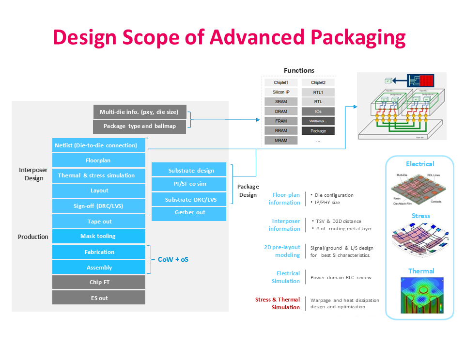
There are new design tasks at the system architecture, die, and interposer levels, and the choices made in these tasks often impact each other. In addition, the challenges of managing the supply chain—involving multiple chiplet suppliers (many of which are themselves small or startup companies working with interposer factories) and managing outsourced semiconductor assembly/test (OSAT) suppliers with advanced packaging capabilities—can become unmanageable. Therefore, system designers must manage this new and more intricate supply chain, facilitating close collaboration and coordination between all parties involved.


New Design Tasks Related to Partitioning

Architectural planning for multi-die systems begins with the purpose, functional description, and performance requirements of the system. However, this task quickly diverges from SoC planning because, early on, the system must be partitioned between different dies.


Partitioning has many parameters. At one level, architects want to ensure that high-bandwidth, low-latency data flows traverse as few die edges as possible and cover as little distance as possible. At another level, designers must partition the system into usable chiplets that can ideally be reused in subsequent designs. Any functionality that cannot be purchased as a chiplet will eventually be implemented in an ASIC. All of these decisions must factor in performance, power, and assembly/test costs.


After partitioning, it’s time to discuss sourcing the die. Third-party vendors should be able to provide off-the-shelf chiplets. However, as design teams have long learned from reusing silicon IP, the right chiplet may not exist. There may be differences in functionality, interface compatibility, and even I/O pad locations, which can cause integration failures on downstream interposers. Sometimes, what starts as a search for the right chiplet ends up with custom chiplet development or repartitioning. There are also practical issues. Finding the right chiplet, and delivering it at the right time, quantity, and price, is a headache.


High-bandwidth memory (HBM) is particularly problematic in this regard. Global demand is tight and is expected to remain so. If a customer does not have a strong existing relationship with an HBM manufacturer, or cannot provide a strong sales forecast, they may face uncertain supply, unstable pricing, or simply no emails returned. Unfortunately, this can also happen with interposer suppliers. Lead times from the three major suppliers can be long and prices can be surprising.


Further Analysis

Chiplet and multi-die advanced packaging bring new analysis tasks to the design backend. The entire assembly must be subjected to electromagnetic field modeling to evaluate the impedance and coupling between interconnects. The assembly must be thermally and mechanically analyzed with accurate dynamic power estimation to check for localized, transient overheating or mechanical stress caused by thermal expansion.


These analyses are particularly rigorous if the application is in automotive or other demanding environments. All of these steps involve tools such as multi-physics analysis programs that are unfamiliar to most chip design teams.


Partners are key

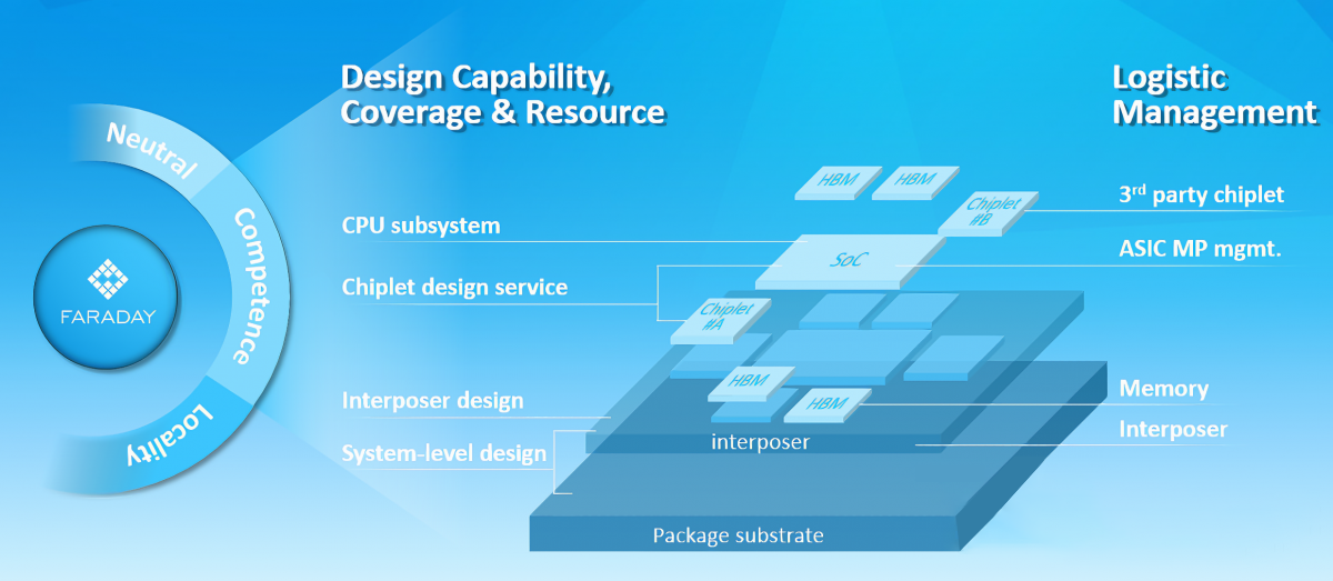
Is the promise of chiplets limited to a few design teams? Although most of the available capabilities are concentrated in major foundries such as Intel, Samsung, and TSMC, other teams can provide chiplet solutions to customers by collaborating with partners who have strong partnerships with these major foundries. In addition, if the partner has expertise in multi-die module analysis, IP, chiplet design, interposer design and manufacturing, and has established strong relationships with foundry and OSAT suppliers, it will be a great help in delivering chiplet-based designs.


Professional design service providers have assembled teams of experts who play a key role in developing chiplet-based system-level solutions. Not only do they have expertise in SoC design, they are also able to handle all stages of multi-die projects - from architecture exploration to supply chain management for large-scale delivery. In addition, these teams are equipped with a full set of internal tools specifically designed to support these complex tasks.


The design service team plays a neutral role in building the project, and they maintain good relationships with major suppliers (chiplets, HBM, ASICs, IPs, interposers, and OSATs) to ensure that products are obtained and the supply chain runs smoothly.


Today, design teams of system developers or small fabless companies can succeed with chiplet-based designs using advanced packaging. This only requires good expertise and partnerships.


  • RFQ